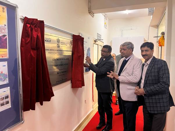
Noida: S. Krishnan, Secretary of the Ministry of Electronics and Information Technology, inaugurated the National Institute of Electronics and Information Technology (NIELIT) Centre of Excellence (CoE) in Chip Design at its Noida campus yesterday. This groundbreaking initiative, in collaboration with SoCTeamup Semiconductors Pvt Ltd, a DPIIT-recognized startup, marks a significant milestone in advancing India’s semiconductor design and development capabilities.
The launch of the Centre of Excellence in Chip Design is aligned with the government of India’s vision to strengthen semiconductor technology and cement India’s status as a global leader in Electronics and IT. The Centre is designed to meet the increasing demand for skilled professionals in the semiconductor and chip design industries, offering state-of-the-art facilities for research, innovation, and training in Very Large-Scale Integration (VLSI) and chip design.
With a vision to lead in semiconductor innovation, the Centre seeks to propel India forward as a global hub for cutting-edge electronics. By providing world-class education, fostering research, and promoting industry collaboration, the CoE is poised to create a highly skilled workforce capable of meeting the evolving demands of the global semiconductor market. This initiative is an essential part of India’s strategy to enhance its position in the international electronics and IT sectors.
During the inauguration, S. Krishnan toured the Centre’s advanced facilities, which include the Project Lab and Smart Classroom. The Project Lab is designed to facilitate collaboration on innovative chip design projects among students, professionals, and researchers. Meanwhile, the Smart Classroom, equipped with modern teaching aids, will provide an immersive and interactive learning experience for students.
In addition, a special demonstration on VLSI-based Intellectual Property (IP) was held, emphasizing the Centre’s commitment to advancing the development of IP in the semiconductor sector. This demonstration highlighted the Centre’s role in building a strong knowledge base in VLSI and fostering a pool of talent to meet the industry’s growing needs.
Bhubaneswar: The Odisha government has stepped up preparations for the disbursement of the fifth instalment…
Bhubaneswar: Thermal hotspots are expanding rapidly across Odisha, with both urban centres and ecologically sensitive…
Bhubaneswar: India on Thursday launched a national framework to facilitate sustainable fishing in the high…
Bhubaneswar: Seeking faster improvements in key human development indicators, the Odisha government on Wednesday intensified…
Bhubaneswar: Eminent linguist and Padma Shri awardee Dr. Debi Prasanna Pattanayak on Wednesday underscored the…
Bhubaneswar: The Odisha Government on Wednesday reviewed the progress of its collaboration with The Convergence…