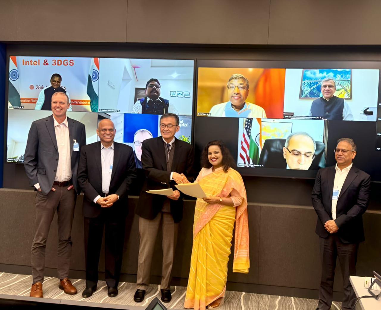
Bhubaneswar/New Delhi: Odisha has received a major boost in its efforts to emerge as a semiconductor manufacturing hub with the signing of a strategic Memorandum of Understanding (MoU) involving the State Government, global chipmaker Intel and US-based 3D Glass Solutions (3DGS) for bringing advanced substrate manufacturing technology to India.
The development was announced by Union Electronics and Information Technology Minister Shri Ashwini Vaishnaw, who described the agreement as a significant advancement for India’s growing semiconductor ecosystem.
“Congratulations to the Government of Odisha, Intel and 3DGS on signing an MoU to bring substrate manufacturing technology to India. This will further strengthen the semiconductor ecosystem in the country,” the Union Minister said in a post on X.
The proposed high-technology manufacturing project is planned in the Bhubaneswar-Khurda region with an estimated investment of nearly USD 3.3 billion. Officials said the facility would focus on manufacturing advanced packaging glass core substrates, high-density interconnect substrates and other critical semiconductor components required for next-generation technologies.
Intel is expected to provide advanced process support and technology expertise for the project, while 3DGS will contribute specialised capabilities in glass-based semiconductor packaging technologies.
According to officials, the project will be implemented in multiple phases over the next five to six years and is likely to create more than 1,800 direct high-skilled jobs. The investment is also expected to generate substantial indirect employment opportunities across the semiconductor supply chain, electronics manufacturing and associated industries.
The agreement further strengthens Odisha’s growing semiconductor footprint following the launch of India’s first advanced 3D chip packaging facility at Info Valley in Bhubaneswar earlier this year.
The project, promoted by 3DGS through its Indian arm Heterogeneous Integration Packaging Solutions, involves an investment of around Rs 1,943 crore and is expected to manufacture advanced glass panel substrates and 3D heterogeneous integration modules used in artificial intelligence, high-performance computing, 5G and 6G communication systems, aerospace, defence and data centre technologies.
At the foundation stone laying ceremony held in April 2026, Union Minister Ashwini Vaishnaw had termed the project a “historic milestone” and highlighted Odisha’s emergence as a key destination in India’s semiconductor and electronics sector.
Chief Minister Shri Mohan Charan Majhi had also stated that Odisha became the only state in the country to host both India’s first compound semiconductor fabrication unit and the first 3D glass substrate packaging facility.
Industry experts believe the latest collaboration will help India reduce dependence on imported advanced semiconductor packaging technologies by building indigenous capabilities in substrate manufacturing and advanced chip packaging.
The initiative aligns with the Centre’s broader push under the Semicon India Programme and the India Semiconductor Mission aimed at developing a robust domestic semiconductor manufacturing ecosystem and attracting global technology investments into the country.